DIY circuit boards

This site may earn a commission from merchant affiliate
links, including eBay, Amazon, Skimlinks, and others.

Spook50

Skål
Supporting Vendor
Joined
Feb 16, 2005
Threads
759
Messages
7,180
Location
Spokane, WA
As the second part of this project I'm working on (once I'm past the R&D and testing portions that is), I want to use it as an opportunity to get some practical experience designing and producing the circuit boards myself. I've done a bunch of research and am comfortable enough with the etching, drilling and tinning processes. I'm still undecided as to whether I want to use the UV development method or the toner transfer method. The UV development method seems to be much more reliable and able to produce high quality traces and pads, but the toner transfer method seems to be less costly and a better way to start when you don't have any of the necessities yet (which I don't).

Any of you who've done your own boards care to weigh in with your thoughts and experiences on the process?

Once I'm up and running this will be 95% a hobbyist thing, but also something I'll use to prototype my own designs before dropping the coin needed to have large quantities produced by a manufacturer.
 
Depends on the complexity of your design, however if your're thinking of going to volume later I would suggest starting out with real prototypes rather than making your own. The industry is capable far beyond what you can do at home and in order to scale up you should be basing your designs off of small SMT parts to control size and volume production costs. If you start out with home built through hole you're still going to have to convert to SMT and run commercial proto's before going to production. Yes, I work in the PCB industry, PM me if you want to talk more about your options.
If you just want to make a few real simple circuits for you and you friends then by all means go for it but don't expect commercial grade reliability from home built PCB's, commercial processes are vastly different from what is done at home.
 
Yeah I've noticed SMT parts are becoming more and more common (and affordable). Given the sizes of the pads and many of the components themselves I definitely believe you when you say it's better to have those professionally done rather than attempt to do it at home. I'd like to do it still on a hobbyist level (just because I think it's kind of cool), but I can see what you mean when you say commercial grade stuff is way better.

I'd love to do home CNC-produced boards, but that's just a pipe dream at this point :D
 
There are a number of places that do "short runs" for a reasonable price.

I would recommend you look at a program called DipTrace, it's free and works well enough that I have done production RF boards with it. It will output the CAM files (Gerber, NC drill) you will need to have a PCB built.

For prototype boards save some cash by skipping the solder mask and silk screen.

It's worth developing the skill to build your own PCB's anyway for those times when you just need a one off PCB for development or a test fixture. I like toner transfer method but you may need to do some touch up with an etch resist pen before you etch the PCB. For crude boards you can even draw the circuit with an etch resist pen, I've done a lot of test fixtures this way.

BTW I've worked with the LPKF board mill for a number of years. It takes a lot of skill to get good results if you are working with fine traces. Not really a DIY thing unless you want to devote considerable time to learning the machine. Other systems are similar.
 
Last edited:
I haven't looked at more than a couple companies so far for small batches, but I didn't realize you can skip out on the solder mask and silkscreen layers for cost savings. That's a big plus.

DipTrace looks pretty badass at first glance (watching the videos on the site now). How would you compare it to Ultiboard as far as interface and capabilities? I have the 11.0 academic versions of Ultiboard and MultiSim. Haven't done anything advanced yet with MultiSim, and I haven't even touched Ultiboard yet (or any serious PCB design software), so I'm curious to hear what more experienced folks prefer in that department. I'm lovin the hell out of MultiSim though. Still got a long way to go, but I'm picking it up :D From what I see on the videos of DipTrace, I'm going to give that a try too. I figure the more I learn, the better off I'll be down the road.

I've seen some of the CNC stuff that folks have done in-home and some of it is mindblowing. But then I see how much the equipment costs and yeah, between that and the time it takes to build up a workable knowledge of CNC software and coding, that'd be a LONG way down the road for me.

Just looked up the LPKF out of curiosity. I like it. Can I have yours? :D
 
Last edited:
I haven't used the programs you mentioned. I do know diptrace is easy to learn, has great support and a forum which offers support.

No you cannot have my LPKF:flipoff2:
 
I haven't used the programs you mentioned. I do know diptrace is easy to learn, has great support and a forum which offers support.

I am LOVING DipTrace. Right now I'm just having fun with it and learning the basics, but you aren't kidding that this is a great program.

No you cannot have my LPKF:flipoff2:

Well it was worth a try :D
 
Yeah I've noticed SMT parts are becoming more and more common (and affordable).

Many modern components are ONLY available in SMT. It has nothing to do with more common and affordable, they are often the only option and they often are CHEAPER (certainly more available) since the package is smaller. PCB cost is by the square inch etc - so using SMT saves money on board real estate.

SMT doesn't waste PCB space and routing channels since you don't need a thruhole for every 'pin'.

There is really no reason to NOT use SMT these days and with a cheapo hand held hot air tool and commonly available easy profile solder paste, it is easy to assemble reasonably fine pitch components. I commonly solder prototype designs with IC's with 0.5mm pitch leads.

Plenty of PCB shops where you can send gerber files and get some boards made for $100 or less, even with soldermask and silkscreen - there's plenty of competition out there to keep the prices reasonable.

cheers,
george.
 
I SMT better, easier to layout , easier to build, easier to rework.

Sent via the ether from my candy bar running ginger bread
 
Check out www.expresspcb.com

I use it all the time for prototype circuits. Here is a board I just made..

pcb.jpg
 
So what's it going to? :D

I've used ExpressPCB a bit and it seems like a good program for the most commonly used features and layouts. My problem is that if I learn one program, it plays hell with me when I try to learn another because I'm so used to the first one. I'm slowly picking up on DipTrace, but I've still got a long way to go. Still having trouble creating proper spec components for some of the circuits I'm trying to do up. Alot of the components I see on there are just far enough off (or I just can't find an equivalent) that I can't use what's already available and have to create custom ones (all to use with the SMT based boards I'm trying to design).
 
Eagle PCB is a popular package for many folk. Having a cad program that generates gerber files will allow you to choose your PCB house versus using a tool that locks you to one vendor.

I use PADS but that isn't 'cheap'.

As you are finding, creating/maintaining libraries for the components you are using is what will lock you into a particular CAD package since you will invest much time in creating your library. Once created and you've made boards, you then have a proven library component and the more you prove, the less likely you want to go through that cycle again and then you are locked in.

So, choose your PCB cad program wisely unless you are just tinkering...

For more complicated designs I use a layout contractor - easier on my sanity and he has the experience (and patience) for multlayer boards :)

Here's a recent design I completed (layout contractor used PADS to do the board), 8 layers, bottom side has the majority of the discretes.

ct8311.jpg


cheers,
george.
 
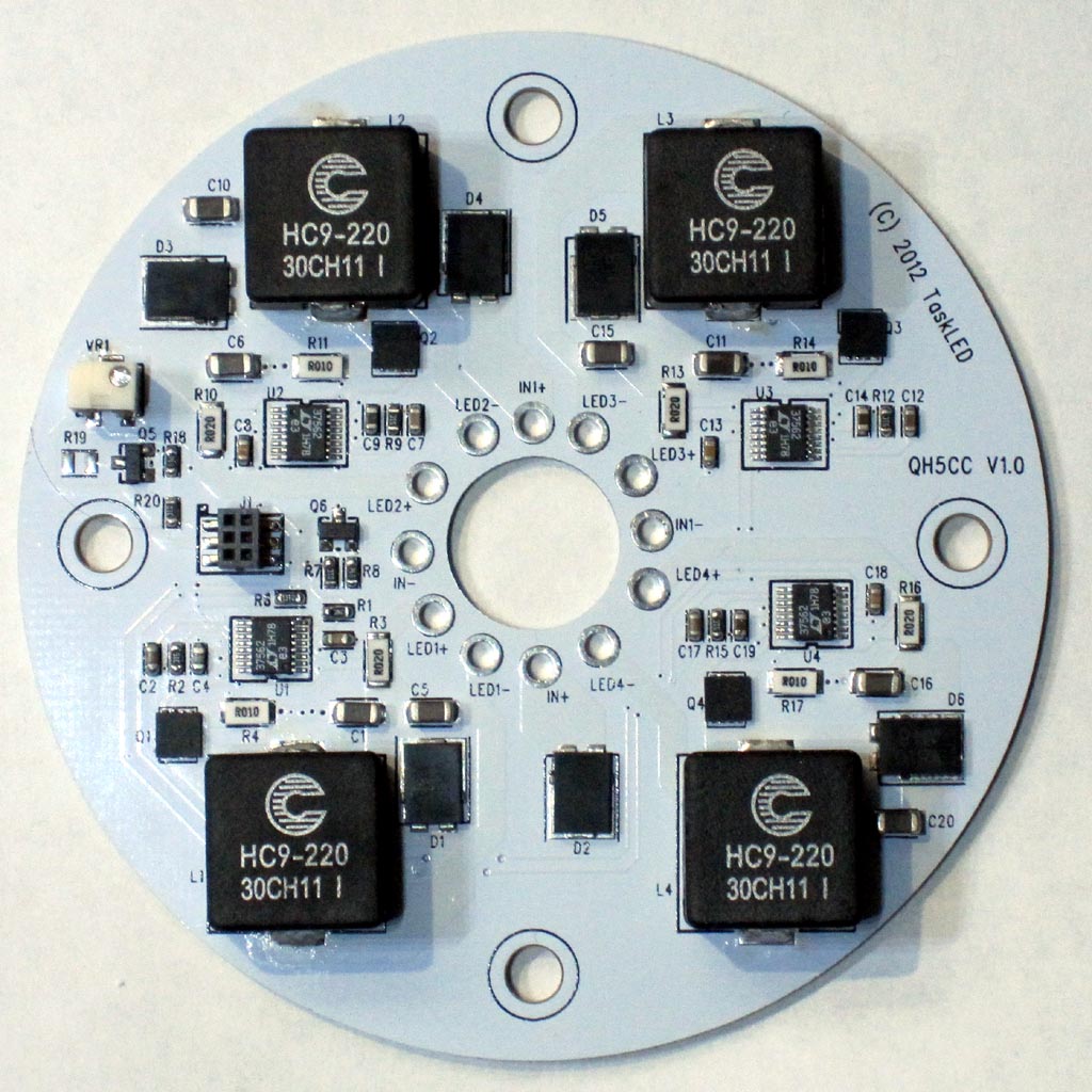
And here's a board I designed last year and routed with PADS. The PCB was fabbed at one of the many fab shops that send off to various places in asia. Typical turn around is 1 to 2 weeks delivered from providing them gerber files.

This is a hand assembled 2 layer board using solder paste and hot plate & hot air tool. It's basically a custom 4 channel current regulated LED driver than can comfortably handle up to 80W of LED load per channel.

qh5cc.jpg


cheers,
george.
 
Pads is a good program.
Protel, now owned by Altium, worked great.
Tango, Highwire, etc etc.
After a while you get use to switching programs.

Concentrate on learning the fundamentals, they will apply to whatever program you use.

1- ALWAYS start with a schematic.
2- ALWAYS take time to build your own, accurate, library.
3- ALWAYS double check the auto router, do a point to point against the schematic on paper with a high lighter.

Actually learning how to jump from one program to another is an asset in itself, be it PCB layout, CAD, CAM, data base programming or whatever. Just remember that all programs in a genre will offer the same features, you just need to learn how to access them in each package.
 
I'm slowly getting comfortable with the schematic aspect of the CAD programs. So far I've been primarily using MultiSim and DipTrace. It's taking some effort, but I keep learning little tricks that have been helping. Creating new components with exact needed specs is still kicking my ass, but I'm getting there.

With any luck I can finalize my first project soon and start getting some SMT boards done up for real world prototyping.
 
@Spook50: I think it is really a good idea if you will use UV development method because it is not much costly and we can try it at home as you can use the lamp as a source of the UV rays or you can build your own UV source with the help of UV LEDs. Therefore, it is an economical and better way of the PCB development.
 
I just built my first toner-transfer pc board yesterday. it was fun.but the home clothes iron - that's a really ugly hack. I can't see how you can get reliable and consistent results this way.

I'm willing to spend a little bit on a heat press. but I don't know much about them or even what temperature and pressure I'll need to get this to work well.
 
I'm going to give the UV method a try for doing small projects. Just have to get a few extra bucks for the supplies and see if I can find any locally.
 
I just built my first toner-transfer pc board yesterday. it was fun.but the home clothes iron - that's a really ugly hack. I can't see how you can get reliable and consistent results this way.
The answer is that you can't. Toner transfer is great for one off boards that are not overly complex, make three to yield one. I still like the method, you just need to realize it's limitations. The photosensitive etch resist method will give you repeatability if that is what you need, as I mentioned earlier in this thread there are also a number of short run PCB manufacturers if you want really professional results.
 

Users who are viewing this thread

Back
Top Bottom